Lab facilities
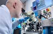
CITC’s lab facilities include equipment for back-end assembly, advanced packaging, additive manufacturing, and testing and analysis. Our lab also serves as demo and application lab for new types of equipment and materials.
Besides our own lab facilities, we have access to the lab facilities of several TNO locations and Delft University of Technology, primarily for wafer-level processes.
This includes the facilities of TNO Holst Centre in Eindhoven and the Else Kooi Lab of Delft University of Technology.
Back-end assembly
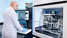
Located at CITC, Noviotech Campus in Nijmegen
- Access to all processes for lead frame packaging
- Flexible labs for high-mix, low-volume assemblies
- Die/clip attach expertise in pressure-less sintering and soldering
Equipment available for
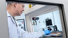
- Material deposition
- Pick and place
- Sintering and reflow
- Wire bonding
- Wafer dicing and laser cutting
- Molding and cleaning
- Optical alignment
Advanced packaging line
Located at TNO Holst Centre, High Tech Campus in Eindhoven
- Compatible with 352x320 mm panels and smaller, including wafers, temporary bonding, and mechanical and laser debonding
- Access to spin and slot die coating, maskless and SCIL imprint lithography, metallization (sputtering/e-beam), PVD, CVD, RIE and barrel plasma etching
- Roll and vacuum lamination
- Access to new tooling concepts like Impulse Printing®
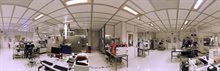
Available equipment
- Advanced panel packaging line
- Impulse printing, laser die transfer
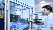
Testing and analysis
Located at CITC, Noviotech Campus in Nijmegen
- Access to standard characterization for lead frame packaging
- Non-destructive and destructive testing
- Perform thermal and electrical testing
- Reliability testing; thermal cycling and shock
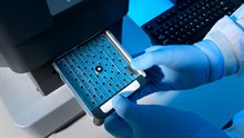
Equipment available for
- Non-destructive inspection
- Optical inspection
- Cross-sectioning/Scanning Electronic Microscopy
- Electrical and thermal testing
- Reliability testing
- Mechanical testing
TNO testing and analysis equipment
Located at several TNO locations in the Netherlands
- Chemical labs with access to DTMA, TGA, rheology, etc.
- Metrology for advanced packaging like SEM and TEM
- RF characterization at specialized RF department