Kick-off Semiconductor Packaging course 2026
A full house today for the start of the CITC Semiconductor Packaging Program! Thirty participants – from countries as far away as Panama and Turkey - have enrolled in the seventh edition of this comprehensive program and have now begun the first sessions of a seven-day program.
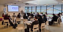
The first topic of the day was an extensive introduction to the fundamental steps of assembly and packaging, with a focus on die-attach technologies.
Lecturers from industry
Two industry professionals, each with many years of experience in packaging technology - Mark Luke Farrugia from SCIPTech and Hans Kuipers from itec - kicked things off by discussing the packaging fundamentals. This was followed by an exploration of topics including the packaging assembly flow, die-attach requirements, integral back-end flow and other die-bonding technologies.
Intensive program
To conclude the first day, Jarno Bots from Neways Electronics will talk about encapsulation technologies such as glob top, transfer and compression molding, map molding, MEMS, and sensor encapsulation. According to program coordinator Ruben Pranger, this day is an intensive start to a week-long series of lectures covering everything related to semiconductor packaging.