First-ever FOPLP demo in the Netherlands
November 6, 2025 – In close collaboration with Holst Centre, CITC has developed a fan-out panel level packaging (FOPLP) process. This is showcased in the first-ever FOPLP demo produced in the Netherlands.
Cost-effective platform
FOPLP is a cost-effective platform for high-performance small form factor packages. The CITC/Holst Centre panel measures 320 x 350 mm2. The technology forms the basis for further development and prototyping, as it serves as a building block for innnovative applications such as communication, radar and autonomous driving.
Test and collaborate
Now that the technology is available in the Netherlands, companies can test it and collaborate with us in Nijmegen and Eindhoven.
November 4, 2025 – Last week, the practical week of the Semiconductor Packaging University Program took place. Three eager students, all industry professionals, worked in our labs and learned that dies can actually fly.
Introduction to packaging technologies
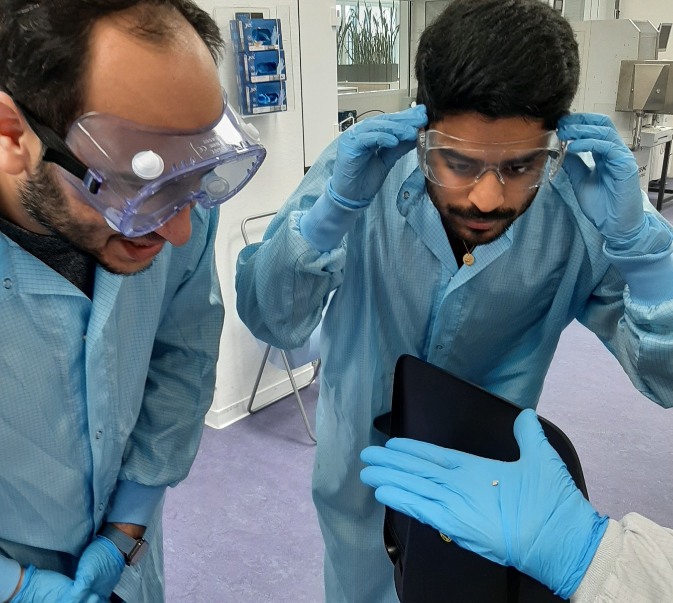 Course coordinator Ruben Pranger introduced them to several conventional packaging technologies, such as die attach, wire bonding, die shearing (see pictures on the right) and die incapsulation. After a week of hard work, the students’ efforts were rewarded with a well-deserved certificate and personalized keychain with chip.
Next edition
The next edition of the Semiconductor Packaging University Program will start in September 2026.
October 21, 2025 – On October 20, CITC and Neways Electronics International NV took an important step in the POLARIS-NGF program theme ‘Valorization – Technology Providers’. This theme focuses on transforming groundbreaking research into competitive industrial solutions.
Joint focus
While CITC provides in-depth research expertise in advanced packaging and die-attach technologies, Neways translates these innovations into manufacturable, reliable solutions for real RF applications. Our joint focus is on sintering, a high-performance die-attach technology with enormous potential for radar and MRI systems, and later for broader applications.
Valorization
By combining research-driven insights with industrial capabilities, we aim to:
- Validate sintering for RF demonstrators
- Accelerate technology readiness from lab to production
- Strengthen strategic autonomy of the Dutch microelectronics ecosystem
This is what valorization means: bridging the gap between knowledge and market, thus creating impact for industry and society. We will get back to you once we have moved from trials to demonstrators – stay tuned.
PRESS RELEASE | Nijmegen, the Netherlands | October 20, 2025
Chip Integration Technology Center (CITC) will become part of TNO. This strategic move marks a significant step toward ensuring the long-term continuity and stability of CITC’s research and operations. The integration emphasizes TNO’s ambition to take a leading position in the innovation of chip packaging technologies and strengthen the regional semiconductor ecosystem in Nijmegen.
“In the coming years, TNO aims to play a key role in the development of advanced chip packaging in the Netherlands,” says Arnaud de Jong, director of High Tech Industry at TNO. “By integrating CITC into TNO, we can intensify and expand our research efforts. We also contribute to the further development of Lifeport in Nijmegen as a strong, future-proof semiconductor ecosystem.” With the investment in CITC, TNO connects chip technology activities between Nijmegen and other semiconductor hubs such as Eindhoven.
Advanced chip packaging
CITC was founded in 2019 by TNO and Delft University of Technology (TU Delft), among others, as an independent innovation center for advanced chip packaging technology. Within an ecosystem of companies, research institutions and educational organizations, CITC has developed into a broad R&D hub that collaborates on technological breakthroughs in advanced chip packaging.
“CITC’s integration into TNO marks a noteworthy moment for CITC. This step underscores our shared vision for the future of chip integration and packaging technology,” says Jeroen van den Brand, general manager of CITC in Nijmegen. “This provides room for growth, accelerates innovation, and strengthens CITC’s international position as a center of expertise for chip packaging.”
Strategic choice for Nijmegen
CITC’s integration into TNO will formally take effect on January 1, 2026. CITC will become part of TNO’s High Tech Industry business unit and will remain located at the Noviotech Campus in Nijmegen. Toni Versluijs, chairman of the CITC Supervisory Board: “CITC continues on its current course. For the Supervisory Board, it is essential that, with TNO’s ambition and investment, we secure continuation of the CITC activities, while building on the existing talent and technology and give CITC room to grow further.”
Lucas van Vliet, member of the CITC Supervisory Board on behalf of TU Delft: “The collaboration between TU Delft and TNO within CITC will change form as of January 1 but remains as strong as ever. TU Delft believes in the importance and growth potential of chip packaging and sees incorporating CITC into a strong organization like TNO as an opportunity to further accelerate innovation in chip technology.”
– ENDS –
About CITC
CITC is a non-profit, joint innovation center specializing in heterogeneous integration and advanced chip packaging technology. With the aim of bridging the gap between academia and industry, CITC has created an effective ecosystem where companies, research and educational institutions collaborate. CITC was founded in 2019 with strategic partners TNO and Delft University of Technology and is supported by the province of Gelderland and Nijmegen municipality. Located on Noviotech Campus Nijmegen, CITC is perfectly situated in the heart of the Dutch semiconductor industry.
www.citc.org
About TNO
TNO is the largest independent research and technology organization in the Netherlands and one of the largest in the EU. We innovate, investigate, and orchestrate, collaborating closely with governments, universities and the private sector. We inform government on policies and empower evidence-based decision-making through rigorous investigations, cutting-edge scientific insights, and reliable measurements. By building national and international consortia and ecosystems, we drive technological and methodological breakthroughs that help to realise a secure, sustainable, healthy, and digital society, and strengthen the earning power of the Dutch economy.
www.tno.nl/en/
Contact
Christian Ketelaars, Communications Manager
E christian.ketelaars@citc.org
M +31 (0)6 48 15 42 92
September 23, 2025 – Just like last year, we had a lot of fun at the Nijmegen Technology Day.
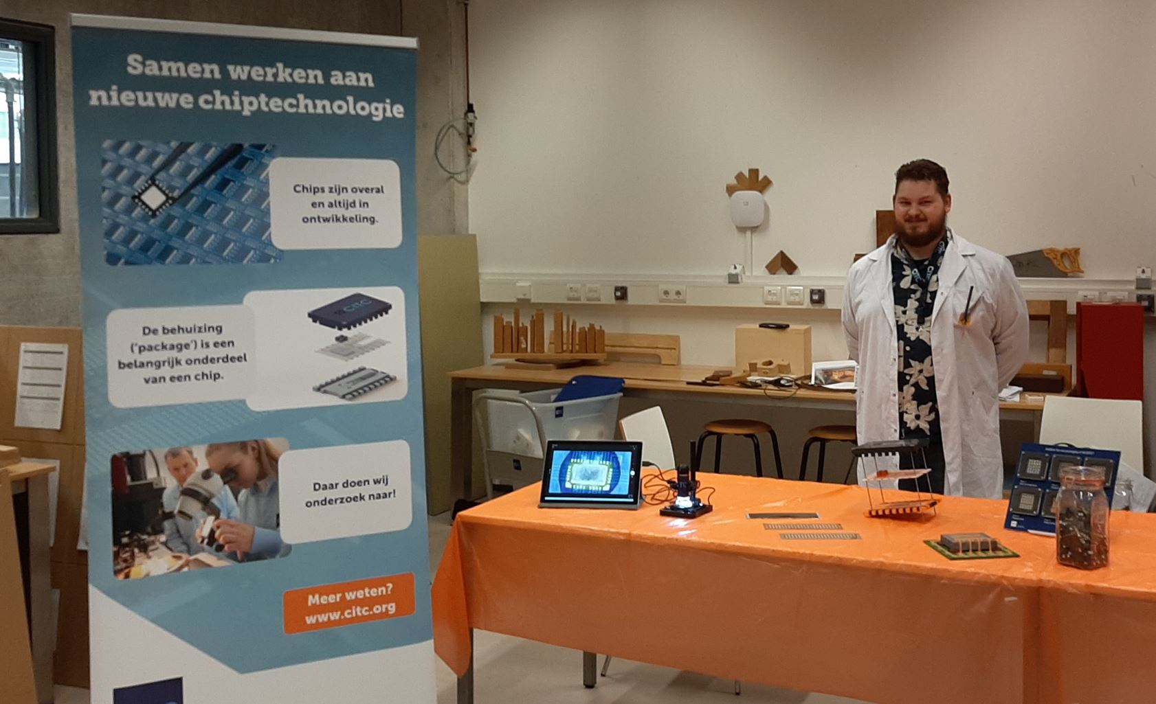
A couple of hundred children and their parents gazed in amazement at the tiny chip under the microscope, tried to guess the number of chip packages were in the jar, and got to work on the ‘make-your-own-microchip-out-of-paper’ craft project.
‘STEM seed’
Several youngsters among these visitors were very impressed, so hopefully, a little ‘STEM seed’ has been planted.
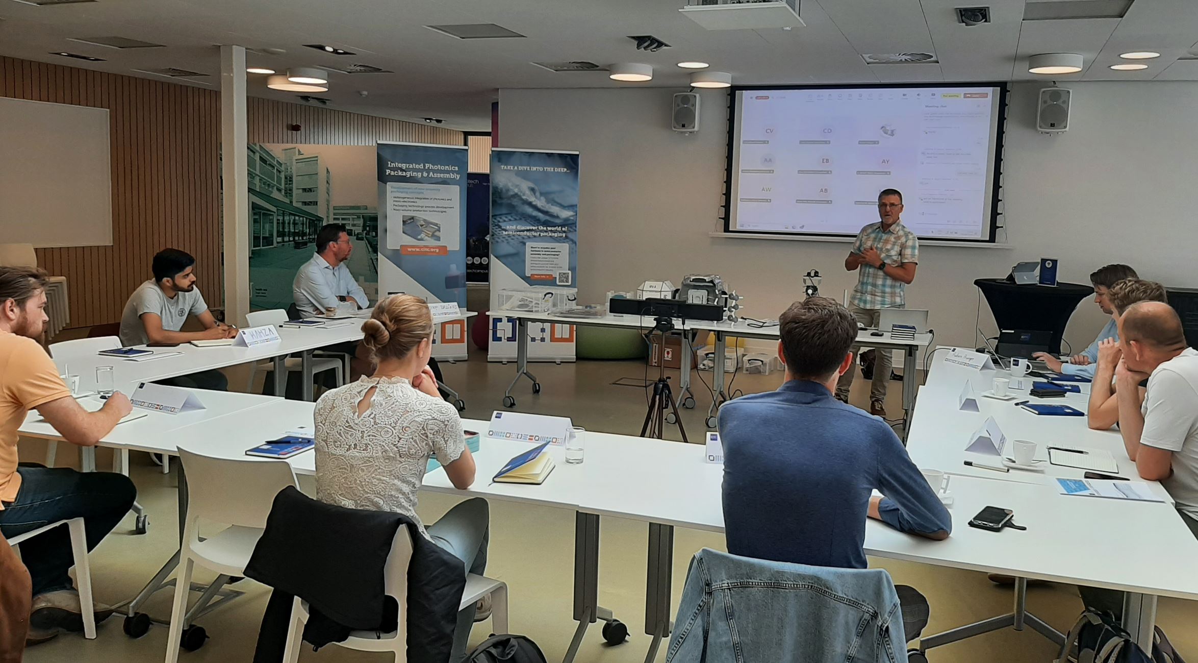
September 2, 2025 – Always a memorable moment: the kick-off of our Semiconductor Packaging University Program. This year marks the sixth edition, and for the first time, it is not Joop Bruines but Ruben Pranger who is coordinating the program.
 Start with front-end technologies
In his introductory speech, Ruben welcomed the participants who attend the program either online or in person at the Noviotech Campus. The first lecturer of the series, as always, is Henk van Zeijl from Delft University of Technology. He will introduce the partipants to the world of semiconductor front-end technologies.
With this knowledge, the next steps in the program will consist of classical and advanced back-end technologies.
We wish all students an enjoyable and interesting time!
June 27, 2025 – Today is Alex Harper’s last day at CITC. Last week, he successfully presented and defended his work at the HAN University of Applied Sciences. His work on the new design of a slit nozzle was graded with a 7 – an above average score according to the examiners.
Former Semiconductor Packaging minor student
Before Alex started as an intern at CITC, he followed the CITC/HAN minor Semiconductor Packaging. Apparently, the topic of chip packaging appealed to Ales enough to make him apply for an internship. Under the supervision of Frans Meeuwsen, Alex developed and tested several new designs for slit nozzles.
Congratulations Alex on this achievement – hopefully, you will also pass your final theoretical exam so you can call yourself a bachelor in Mechanical Engineering. We wish you all the best!
June 25, 2025 – CITC participates in the QuLight Detection project. The aim of this project is to develop a single photon detector (SPD) that is significantly more scalable than existing detectors. This SPD will be used in quantum computers, which allows for significant upscaling.
 No cryostats required
Our SPD is based on a highly efficient single photon avalanche detector (SPAD). Unlike SNSPDs, SPADs do not require cryostats for operation, which leads to:
- a tenfold decrease in energy consumption
- a thirtyfold reduction in size, and
- a tenfold decrease in cost.
Electrical and optical integration
In this project, CITC is responsible for the electrical and optical integration of the SPAD sensor. CITC will develop the packaging concept, which consists of mounting on an interposer using flip chip and low-loss optical coupling between SPAD sensor and glass optical fiber. CITC will assemble multiple prototypes that are ready for integration into the detector modules.
The results of the QuLight Detection project strengthen both the knowledge base and the economic position of the eastern Netherlands. In doing so, we create a robust environment for high-tech innovation and collaboration with industry.

June 24, 2025 – CITC’s Noud Schoenmakers was one of the presenters at the Mechanical Engineering (ME) Innovation Day at Eindhoven University of Technology. He talked about his PhD work on understanding the micromechanics and reliability of lead-free interconnects designed for power packaging.
Creating impact
The ME department wants to create impact through the innovations resulting from their research. An important route to achieve this is through valorization by collaborating with industrial partners linking their (fundamental) research to practical applications for the real world.
To acknowledge the importance of innovation and valorization, the ME department hosted its first annual Innovation Day, dedicated to showcasing how its research creates and fosters societal and industrial impact.
June 17, 2025 – What a great day we had when we visited the Technasium students of Mondial College last Friday! All students took the assignment (create a chip exhibit that can be used at the upcoming Nijmegen Technology Day for children aged 8-12) very seriously and presented the most amazing projects.
Difficult decision
 The jury had a hard time deciding which team had created the best exhibit; there were memory games, escape rooms, a ‘chip-o-maat’ and very intricately built electrical circuits. It was clear that the students learned a lot about chips and their packaging, but also about binary codes, programming, laser work and so on.
This is what STEM education is all about, we look forward to next year!