
Practical program starts with Panamanian participants
October 25, 2023 – The practical part of the CITC/HAN Semiconductor Packaging University Program started last week. First participants: four professors from the Universidad Tecnológica de Panamá.
Earlier this year, CITC’s education consultant Joop Bruines was invited to give a presentation in the virtual conference cycle about R&D of the Universidad Tecnológica de Panamá. As a result, several Panamanian professors and PhD students showed interest in the Semiconductor Packaging University Program.
Getting up early for online classes
Four participants joined the online theoretical part that started in September online. “It meant getting up really early for us, but it was worth it”, says Diego Bouche. “We did not know much about the semiconductor industry and now we were at least prepared for our visit here.” Together with three colleagues Diego arrived in the Netherlands for a week of practical training.
Visiting semicon companies
One of the other participants, Itamar Harris, explains the background of their visit. “The U.S. is interested in locating one or more semiconductor OSATs in Panama. We want to be well prepared and are happy to be able to take a look at the semiconductor industry in Europe.” There was plenty of opportunity for this, as Joop had arranged several visits to semiconductor companies on the Noviotech Campus. In addition to visits to ITEC and Sencio, the group was invited to NXP where they received a plant tour and visited the test program development department.
Working with backend equipment
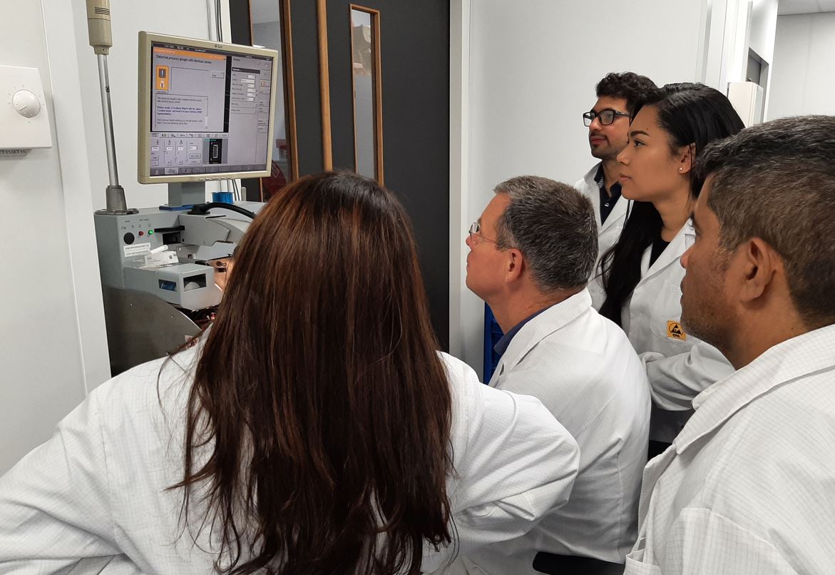 Back at CITC, the group was trained on the backend equipment in the labs. Under supervision of CITC lab manager Martien Kengen, they learned all the basic principles about typical backend activities such as die placement and wire bonding. Diego comments: “What I really liked was that we were actually allowed to work with the equipment. Wire bonding is a very challenging task, so it is good to have experienced this first-hand.”
At the end of the week and after spending many hours in the lab, the four participants received their well-deserved certificate from Martien and Joop.
Up next…
The practical part of the CITC university program continues this week with European based participants and the students who follow the full minor program at the beginning of November. If you are interested in expanding your knowledge of semiconductor packaging, check out the university program information.