Access to Infrastructure
CITC’s lab facilities support the innovation programs and contribute to education through internships and MSc/PhD programs. Our lab also serves as demo and application lab for new types of equipment and materials. It is also available to third parties to enable them to develop, test and implement new packaging solutions.

In-house facilities
Our lab has all the equipment and tooling for basic packaging assembly technologies:
- Surface (plasma) cleaning/sample preparation
- Dispensing/glue-solder depositing: dispensing, dam and fill, potting
- Die bonding: glue-solder-sinter
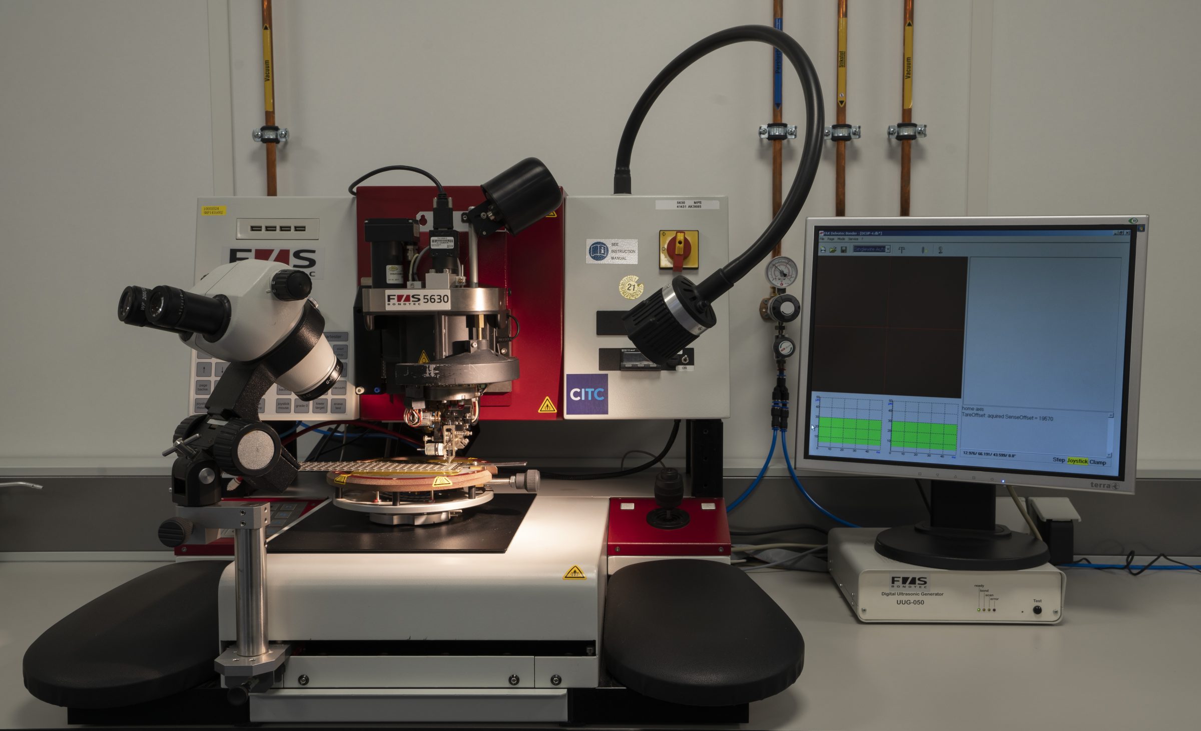
- Wire bonding: wedge-wedge, ball-wedge, Cu, Al
- Optical assembly: active, passive
- Testing: thermal, cross-sectioning, x-ray
CITC has a Smart Industry Field Lab status, which indicates that it is a place where industry and research organizations jointly develop, test and implement smart industry solutions.
Additional external facilities
Besides our own lab facilities, we have access to the lab facilities of our strategic partners TNO and Delft University of Technology (TUD), primarily for wafer-level processes.
This includes the facilities of TNO Holst Centre in Eindhoven and the Else Kooi Lab of TUD.
Assembly processes and technical capabilities
The equipment in our lab allows us to examine the physical aspects of various processes, with the ability to perform fast prototyping for proof-of-principle samples using industrial quality samples. We also have the equipment to test and evaluate the quality of the assembly process.
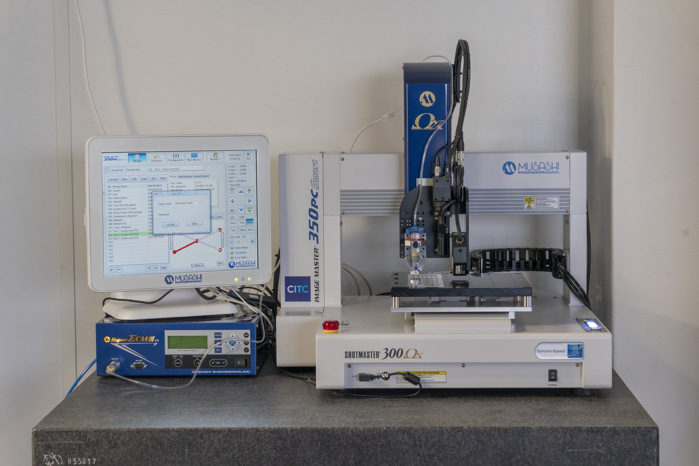
Dispensing/ glue-solder depositing
- High accuracy 3D position and volume control dispensing system
- Manual dispensing system
- Manual stencil printer for fast proto typing
Diebonding
- Pick and place with high positioning accuracy (7µm @ 3 sigma)
- Die attach and flip chip bonding with high positioning accuracy (0.5 µm @ 3 sigma)
- Precise controlled bondforce ranging between 15 gf to 1000 kgf
- Eutectic bonding under shielding gas (N2, forming gas)
- Thermal-curing, vacuum and solder reflow ovens
- Pick and place from waffle tray
Wirebonding
- Flexible workholder to handle large spectrum of different substrates and packages
- Deep access fine wire wedge/wedge bonder for 18-75 µm Al and Au wire
- Ball/wedge bonder for 18 – 50 µm Au wire
Optical assembly
- Active optical alignment station (alignment accuracy typical 0.02 dB)
Testing
- Die shear tester, ranging up to 200 kgf
- Wire pull tester up to 100 gf
- Temperature cycling chamber (-70 to +180°C, max 20K/min)
Surface cleaning/sample preparation
- Bench top plasma cleaner, suitable for a wide variety of plasma cleaning, surface activation and adhesion improvement multiple gasses, e.g. O2, Ar, H, He and fluorinated gasses
- Ultrasonic bath cleaner
Rapid pcb prototyping
- Easy transformation of electronic design to prototype pcb
- Single or double layer pcb, max. 128 x 105 mm