
Spotlight on reliability lab activities at CITC
October 30, 2023 – Reliability. According to our Ph.D. researcher Henry Antony Martin, this is an essential performance metric in realizing high-efficiency, high-power density devices. In his work, Henry mainly focuses on reliability monitoring and thermal management.
He explains: “Nowadays, we are very aware of environmental problems and the need for sustainability. This awareness has made energy-efficient systems, renewable energy technology, electric cars, and smart grids more important. To ensure that these systems work well and last long, reliability is the key. It’s the ultimate guarantee that the systems continue to work and perform as they should.”
Extensive lab infrastructure
Henry continues: “At CITC, we are committed to supporting the packaging community with our execution excellence in advanced semiconductor and photonic packaging innovation and assembly processes. With reliability testing, we gain quantitative insights into our packaged products and evaluate them to improve the packaging processes.”
CITC has an extensive laboratory infrastructure with equipment for reliability testing/monitoring methods, characterization, and advanced imaging techniques:
- Thermo-mechanical cycling lifetime testing
- Probe stations for PQFN
- Advanced imaging techniques
Thermo-mechanical cycling lifetime testing
Conducting accelerated lifetime tests for packaging components is essential in reliability engineering. The thermo-mechanical cycling lifetime (TMCL) testing framework allows CITC to rigorously evaluate the durability and long-term performance of micro and power electronic packaging components.
Henry: “Such accelerated TMCL testing is usually performed offline with packaged devices that are measured intermittently. However, we have the unique capability to conduct both offline and online condition monitoring during TMCL testing. Online monitoring of device condition includes characterizing electrical and thermal performance at different ambient temperatures to effectively evaluate package performance degradation.”
Probe stations for PQFN
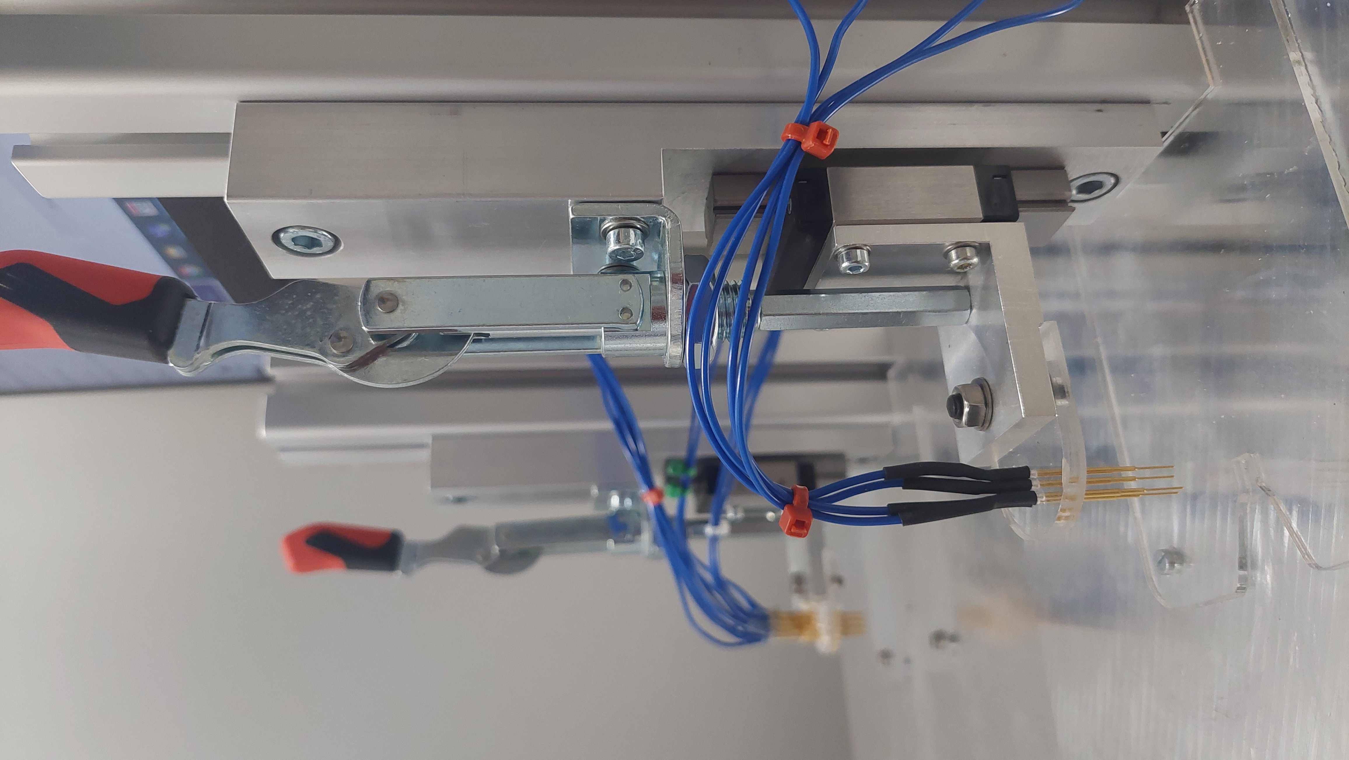 Testing and characterization of surface mount devices (SMDs) require soldering on printed circuit boards, which can result in bottlenecks when conducting through-acoustic scans for package analysis. Therefore, for research purposes, CITC has developed custom probe stations* capable of directly probing SMD packages without the need for soldering to a test board.
“Currently, we have two different probe stations that are designed specifically for two different SMD package types,” adds Henry. “The probes allow 4-point Kelvin contacts for accurate measurements and are connected to a dual-channel source unit and a digital multimeter. The instruments are controlled using a user-defined MATLAB program and collect the data for further processing.”
*manufactured by our partner Holst Centre
Advanced imaging techniques
To effectively analyze failures and improve packaging processes, CITC has equipment such as confocal laser microscope(s), scanning electron microscope (SEM), and scanning acoustic microscope (SAM).
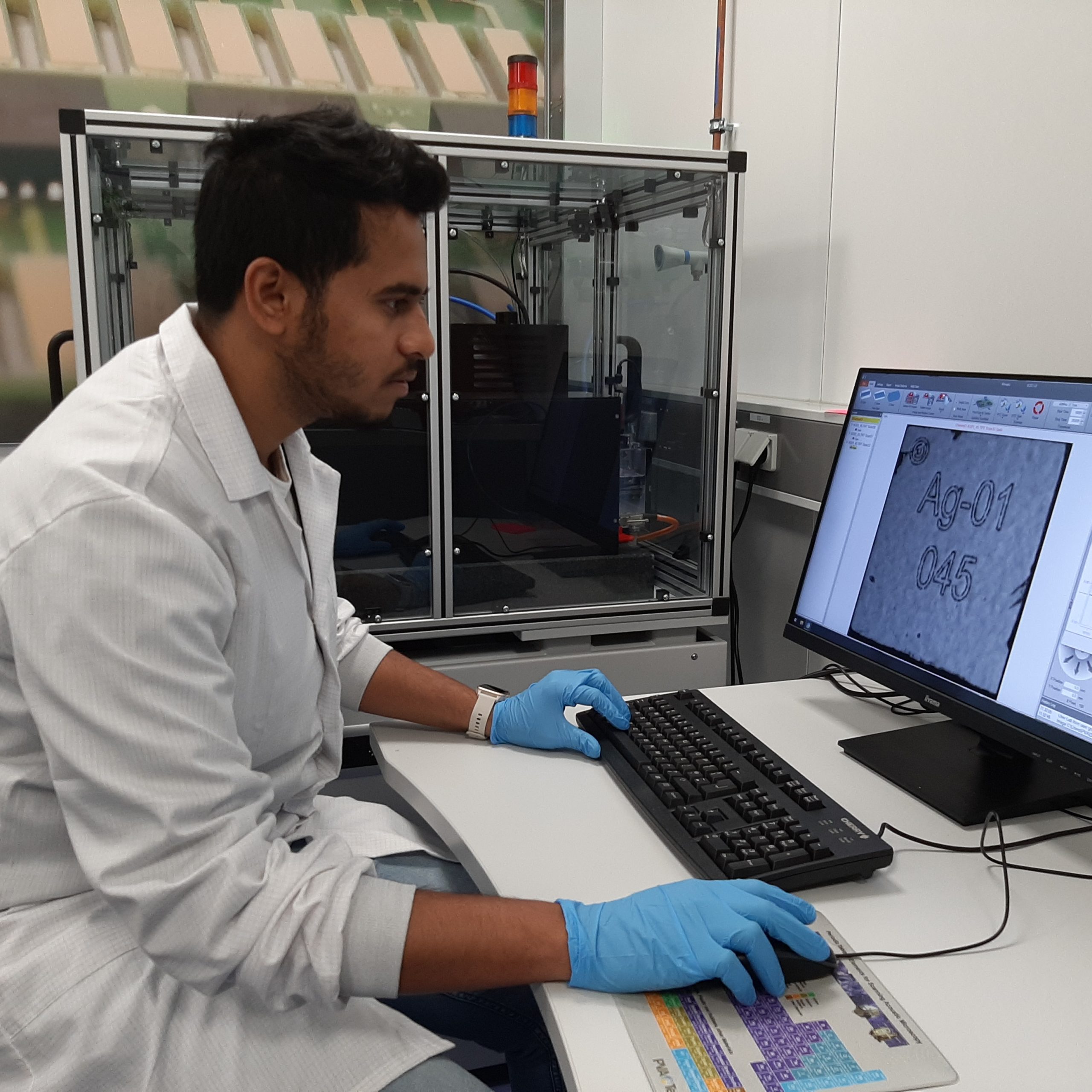 Henry has spent a lot of time working with the SAM due to its importance in package reliability analysis. He explains why he considers it so useful: “Scanning acoustic microscopy is a powerful, non-destructive method for identifying electronic packaging defects. Acoustic microscopy consists of a piezoelectric transducer that generates ultrasound pulses that are transmitted to the sample through a water medium.
Water is used as a coupling medium in SAM due to its excellent ultrasonic conductivity and relatively low acoustic impedance. As the ultrasonic waves interact with material interfaces, they undergo reflection and scattering, producing an echo signal that is converted into an electrical output. An image processor then digitizes this signal. The raster scanning motion of the acoustic transducer generates ultrasonic pulses at high frequencies that are reflected from the sample, thereby capturing the depth information.”
He continues: “It is important to acknowledge that SAM, like any imaging technique, has its limitations. The penetration depth of acoustic waves typically ranges from approx. 1 mm to 2 mm for most materials and image quality is highly dependent on the properties of the sample being imaged. When designing new package types, and improving the package assembly processes, SAM is essential to understand the failure modes without any destructive methods.”
If you are interested in (one of) these reliability techniques, please contact CITC.