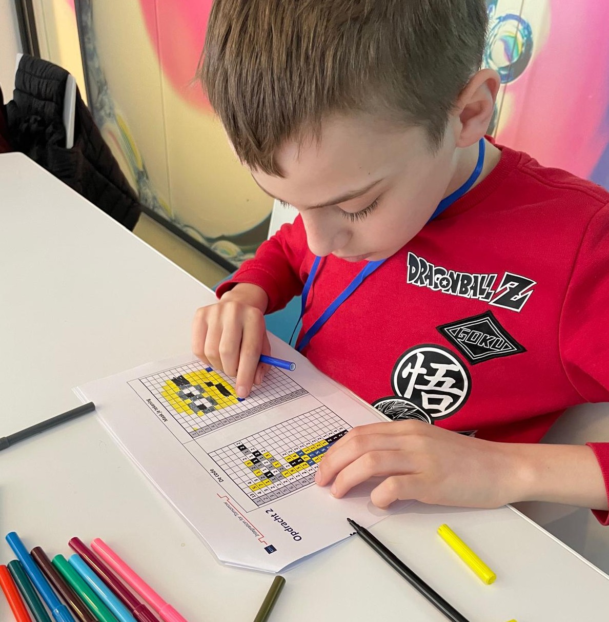
Well-attended Doe Dag at CITC
April 20, 2026 – Last Thursday was the Sterk Techniekonderwijs – Rijk van Nijmegen Doe Dag 2026. Eleven young students visited CITC and were introduced to research into semiconductor packaging.
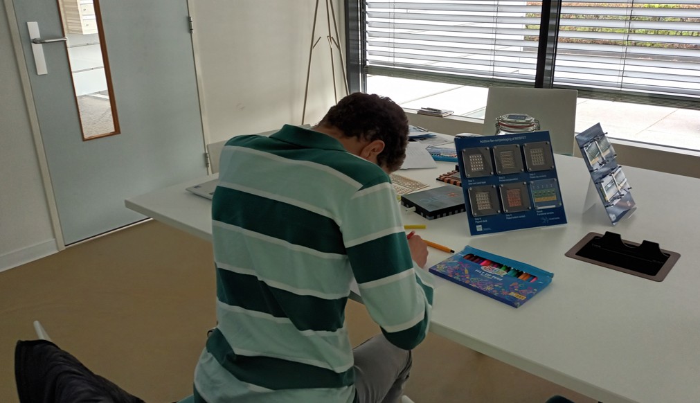
Hands-on assignments
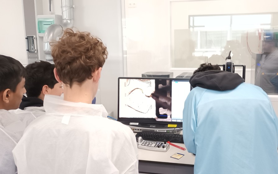 After a brief introduction to packaging, the students worked on an assignment on binary coding and visited our labs. Our technician Bart van Goor had prepared several hands-on assignments so they could literally experience research practice.
Career in science… or not
Although not all students will choose a career in science (“I want to be a chef. Or a journalist, Or something in sports”), more than half of the students are seriously considering a technology degree. Hopefully, we will see them again in the future.
April 15, 2026 – For the third consecutive time, CITC participated in TNO Semicon Day. And what a day it was for our business development manager Ruud De Wit.
Presentation on main stage
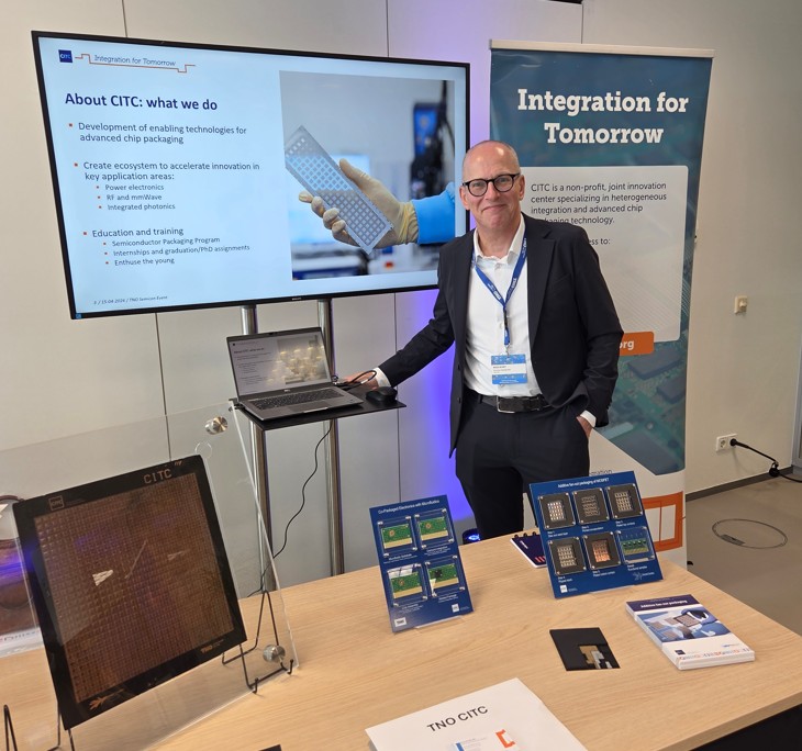 At this year’s TNO Semicon Day, he not only had a booth at the innovation market, but he also took the stage in the main hall.
Together with Tindara Verduci (program manager RF and mmWave packaging) and Edsger Smits (program manager power packaging), he presented how CITC can support the European semiconductor industry with advanced chip assembly, testing and design.
Many thanks to the organizers of TNO Semicon Event – we hope to be there again next time!
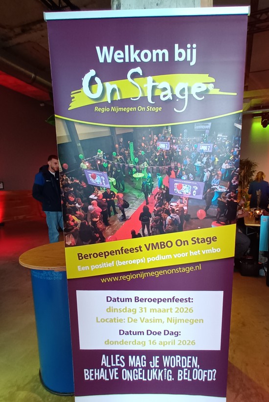
April 1, 2026 – “You can become anything you want, except unhappy. Promised?” That is the appealing motto of regio Nijmegen On Stage‘s career festival. More than 100 companies participated in the festival this year. The target audience: the approximately 1,000 second-year students from vocational schools in Nijmegen.
Future of the Netherlands
The students were welcomed to the festival after a walk down the red carpet and a well-deserved round of applause – after all, they represent the future of the Netherlands when it comes to the practical implementation of many professions in healthcare, the green sector, and technology.
Pursue a career in chip research
CITC was present to inspire the students to pursue a career in chip research. Our enthusiastic team managed to recruit 12 students who will visit us on the upcoming Doe Dag (Activity Day) on April 16.
March 19, 2026 – CITC is pleased to welcome Subba Kedarnath Gupta Vemula as an intern. Over the next six months, he will work on copper sinter pastes and investigate the role of additives and their effect on material behavior.
Materials Science
Subba is currently pursuing a Master’s degree in Materials Science at Technische Universität Darmstadt. During his internship, he aims to gain practical experience and deepen his knowledge of material processing in an applied research environment.
Access to innovation and education
At CITC/TNO, we support students and researchers by providing access to advanced lab facilities and a collaborative environment.
March 12, 2026 – ‘Dear CITC team, you provided a great explanation, and I learned a lot. Most importantly: I enjoyed it very much; thank you!’ What a lovely comment from Nour (11), a participant in the Weekendschool Nijmegen, who visited CITC.
Introduction to chips and packaging
 Along with 29 classmates, Nour spent her Sunday afternoon learning more about chip packaging. The CITC visit followed one to NXP, where the students were first introduced to chips and began programming a microbit.
At CITC, they learned about the importance of chip packaging and what it means to be a researcher. While continuing their microbit project, they also visited the CITC labs and attended a workshop on binary drawing.
‘Tech seed’
The children worked hard and clearly had a good time. According to their teacher, the ‘tech seed’ has been planted – and that is exactly what we had in mind!
CITC aims to provide access to education to everyone, from young children such as the Weekendschool participants to bachelor’s, master’s and PhD Students.
February 10, 2026 – CITC is very pleased to welcome our new business development manager: Ruud De Wit. Although new to our team, Ruud is a very familiar face to CITC, having worked with him for years when he was still at Henkel.
Extensive experience
He brings approximately 25 years of semiconductor back-end assembly experience in global key account management, global product management, and new business development (in die attach, sintering and wafer level encapsulation). Ruud will support CITC’s expanding power and RF semiconductor testing capabilities and new advanced chip packaging developments.
January 27, 2026 – Today’s first edition of Lifeport Regio Arnhem Nijmegen Semicon Event also marked the first time CITC presented itself as part of TNO. We are officially joining forces to strengthen the Netherlands’ position in advanced chip packaging. Additionally, the Provincie Gelderland announced renewed investments in CITC for the period 2026-2030.
Shared mission
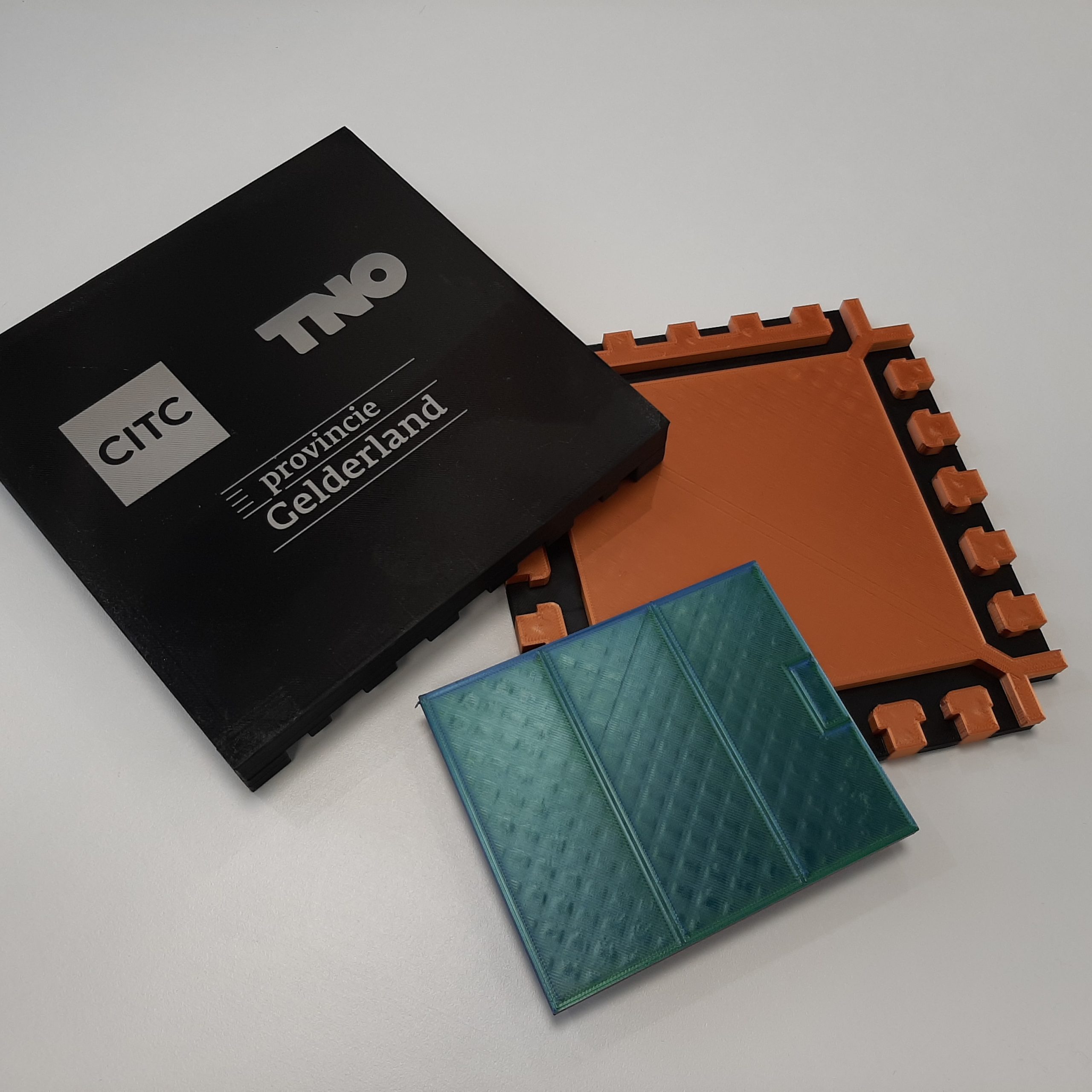 Together, we share a mission for the future of chip integration and packaging technology. During the event the three pieces of the ‘packaging puzzle’ fell into place: CITC as a center of expertise for chip packaging, TNO, which enables us to intensify and expand our research efforts, and the province, as a grant provider, contributing to the further development of Lifeport in Gelderland into a strong, future-proof semiconductor ecosystem.
In the photo below from left to right: Jeroen van den Brand (CITC), Helga Witjes (Provincie Gelderland) and Arnaud de Jong (TNO)
Credit top picture: Rutger van Loo
January 14, 2026 – For several CITC researchers, 2026 started with an extensive three-day training in confocal scanning acoustic microscopy. Andreea Tomita, applications engineer at our partner PVA TePla AG, visited our lab which is equipped with one of their microscopes, to provide a comprehensive training.
Theory and practice
After a morning devoted to the theoretical background of this type of non-destructive testing and quality control, the team went to the laboratory to get acquainted with the microscope. This was time well spent and we plan to use the microscope more often in our research.
A big thank you to the PVA TePla team for organizing this training: Andreea Tomita, Tatjana Djuric-Rissner and Kasim ALTIN.
November 19, 2025 – Our colleague Henry Martin travelled to Caceres, Spain, to attend the kick-off of the SPARK-e project*, funded by the European Union. CITC is part of the consortium organized by CIIAE – Iberian Centre for Research in Energy Storage.
Focus on new materials
The consortium focuses on new materials for advanced energy recovery and heat dissipation in electronics. SPARK-e targets thermal management in increasingly compact and powerful electronic devices, where overheating reduces efficiency and reliability.
The researchers will develop and test solid-to-solid phase change materials that can more effectively regulate heat flow, act as thermal switches, and even convert stored heat into electrical energy through pyroelectric effects.
Co-packaging electronics
Within this project, CITC will focus on co-packaging electronics with phase change materials (PCMs) for thermal switching and thermal regulation. We look forward to working on this together with our fellow consortium members.
*EIC Pathfinder (101221862 SPARK-e)
November 6, 2025 – In close collaboration with Holst Centre, CITC has developed a fan-out panel level packaging (FOPLP) process. This is showcased in the first-ever FOPLP demo produced in the Netherlands.
Cost-effective platform
FOPLP is a cost-effective platform for high-performance small form factor packages. The CITC/Holst Centre panel measures 320 x 350 mm2. The technology forms the basis for further development and prototyping, as it serves as a building block for innnovative applications such as communication, radar and autonomous driving.
Test and collaborate
Now that the technology is available in the Netherlands, companies can test it and collaborate with us in Nijmegen and Eindhoven.